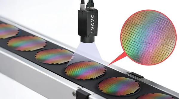
Using AOI (Automated Optical Inspection) to check wafer surface condition and detect metallic residue or scratches is already a mature and widely used method. However, as the semiconductor industry advances toward more cutting-edge processes, inspection standards continue to rise. Traditional visual inspection technologies are facing unprecedented challenges:
-
High resolution requirements
-
Rigid algorithms unable to adapt to complex environmental changes
-
Insufficient accuracy negatively impacting yield
By introducing AI into AOI, you can leverage the strengths of visual inspection while breaking free from rule-based algorithm limitations. Integrating AI not only delivers more accurate detection, but also offers greater flexibility in application.
The Three Major AI-Powered Applications in Wafer Inspection
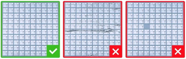
1. Wafer Defect Detection
Semiconductor wafers are composed of multiple layers of precisely deposited materials. This structure makes potential defects both diverse and unpredictable, capable of appearing anywhere on the wafer. One key challenge is that coating defects may exhibit unpredictable color variations, making it extremely difficult to detect them against previously deposited complex background layers. Traditional rule-based vision systems struggle to handle such diversity, resulting in unreliable detection even on multi-layered backgrounds.
DaoAI’s Solution: AI learns from defect-free samples to establish a standard model. Without needing defect examples, AI can detect anomalies that deviate from the norm—completely independent of rigid rules.
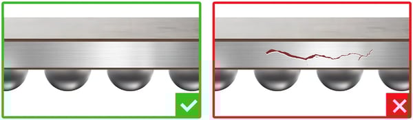
Micro-Crack Detection in WLCSP Sidewalls
Wafer-Level Chip-Scale Packaging (WLCSP) involves multiple layers, and micro-cracks can occur due to mishandling, excessive pressure (during solder ball processing), or transportation mishaps. Rule-based machine vision methods are time-consuming, difficult, and often fail to distinguish between layered changes and tiny cracks.
DaoAI’s Solution: :AI continuously learns from human feedback to gradually understand defect patterns (like micro-cracks), even in cluttered backgrounds and low-contrast situations, and achieves pixel-level precision in detection to meet high-speed inspection requirements.
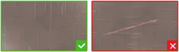
Die Surface Inspection
Defects on die surfaces—such as cracks, fractures, and burn marks—are highly variable in appearance and location. Rule-based machine vision struggles to accurately detect these defects and is often complex and time-consuming.
DaoAI’s Solution::By learning from defect-free examples and without relying on rigid rules, AI can recognize a wide range of coating anomalies and detect cracks, fractures, or burn marks wherever they might appear.
Introducing AI into AOI isn’t just an upgrade—it’s a pivotal step for semiconductor manufacturing to reach higher standards. The strong learning and adaptive capabilities of AI bring unprecedented precision and efficiency to wafer inspection, becoming a solid backbone for ensuring semiconductor yield.
Don’t let traditional inspection technologies become a bottleneck. Let AI breathe new life into your production line, achieving more accurate and efficient inspection and giving you the competitive edge in advanced processes.
Contact us now to get started!