DaoAI PCBA AOI
AI Inspection System
Program, detect, improve, all with AI.
Program faster, detect smarter, and improve continuously
99% Accuracy with AI Algorithms
No Overkill, No Missed Defects
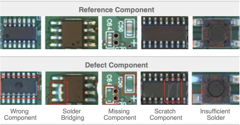
Compared with rule-based or grayscale rule algorithms, Visual AI overcomes missed detections caused by similar colors between the PCB and components. It significantly improves detection accuracy for defects such as missing parts and scratches.

Accurately recognize text on components
PCB Dedicated OCR
AI training are based on real PCBA photos, and it overcomes challenges like blur, damage, dirt, and low contrast
1 ms /component
Millisecond-level Inspection
Instantly detects missing parts, wrong components, and polarity on high-density boards without computing bottlenecks.
CPU/GPU Parallel Processing Architecture
GPU focuses on processing complex defects and OCR, while the CPU synchronously handles logic operations. True parallel processing ensures tasks do not wait for each other, maximizing hardware efficiency.
45 cm²/s
High Throughput
Perfectly matches the rhythm of high-speed SMT lines, eliminating post-reflow inspection bottlenecks.
Complete Modeling in 5 Minutes
No CAD or libraries — one golden sample covers capacitors, resistors, IC pins, and all defect types.
AI Auto-Detects Components and Generates Bounding Boxes
With no coordinate data required, AI automatically maps every component and creates precise bounding boxes within seconds, even for rotated parts, significantly shortening initial programming time.
AI-Generated Inspection Thresholds
AI analyzes the golden sample’s color distribution and automatically generates optimal thresholds, greatly reducing debugging time and speeding up recipe completion.
Smarter and more stable the longer it runs.
Operators can instantly provide feedback to retrain the AI model in real-time. With every new batch of production data, the system continuously improves.
Iterative Learning Loop
Reduces False Alarms Through Feedback Learning
When an operator confirms a false alarm, the AI learns the true characteristics as training samples, preventing similar features from being misjudged again and progressively reducing false alarms.
Offline 2D AI AOI Machine
DaoAI P1 & P2
DaoAI P1& P2 leverages advanced visual AI to automate PCBA inspection programming. By learning directly from golden sample, it auto-detects components, generates bounding boxes, and defines defect thresholds — accelerating setup from hours to 5 minutes.

Introducing DaoAI P Series
Offline & Inline 2D AI AOI Solutions
DaoAI offline and inline 2D AI AOI machines leverage advanced visual AI to automate PCBA inspection programming. By learning directly from golden sample, it auto-detects components, generates bounding boxes, and defines defect thresholds — accelerating setup from hours to 5 minutes.

The High-Mix Dilemma
Overcoming the NPI Bottleneck in Modern Electronics Manufacturing
Unraveling the complexities of modern manufacturing and the elusive promise of the Smart Factory.
DaoAI P1/P2 Specifications
DaoAI P1
5MP0 Camera /month
DaoAI P2
12MP0 Camera /month
DaoAI P1
DaoAI P2
Optical System
Conveyor & PCB Size
Inspection Capability
Additional Functions
Inspection and Auto-Configuration Capabilities
|
Body |
Polarity | IC Leads |
Text
|
|
|---|---|---|---|---|
|
Capacitor |
|
|
|
|
|
Resistor |
|
|
|
|
|
Multilayer Chip Inductor |
|
|
||
|
Aluminum Electrolytic Capacitor |
|
|
|
|
|
Tantalum Capacitor |
|
|
|
|
|
Resistor Array |
|
|
|
|
|
Power Inductor |
|
|
||
|
LED |
|
|
|
|
|
SOT/SOD |
|
|
|
|
|
SOIC/SOP/TSOP/TSSOP/MSOP |
|
|
|
|
|
QFP |
|
|
|
|
|
QFN |
|
|
||
|
TO-263/TO-252 |
|
|


