
高速、高效率
专为现代SMT产线设计

1毫秒/组件
毫秒级检测
即时检测高密度板上的缺失组件、错误组件和极性问题,无运算瓶颈。

45 平方公分/秒
吞吐量
完美匹配高混合量 SMT 产线节拍,消除回流焊后检测瓶颈。

CPU/GPU
平行处理架构
GPU 专注于处理复杂缺陷与 OCR,CPU 同步处理逻辑运算。真正的平行处理确保任务不互相等待,最大化硬件效率。
PCBA 检测设备
全线搭载DaoAI AI AOI for PCBA AI检测软件
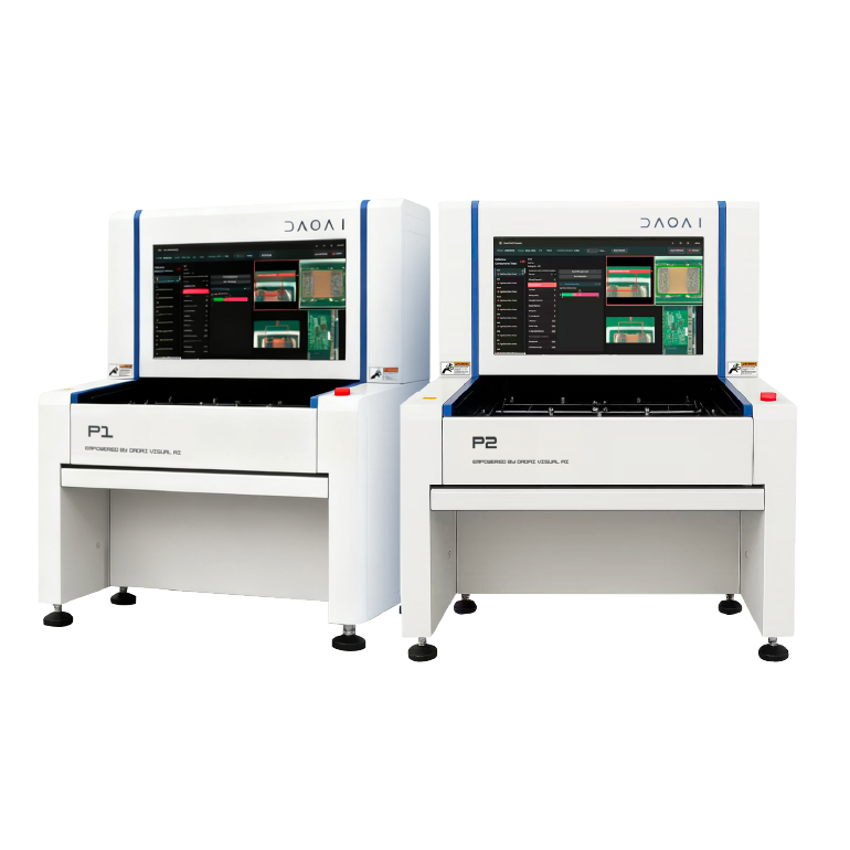
DaoAI P1/P2
离线式 · 手动上料适用场景高混合产量场景
相机/分辨率P1: 5MP(15 微米)
P2: 12MP(10 微米)
P2: 12MP(10 微米)
成像系统10MP 远心光学镜头
光源多光谱 RGB 六信道
最大 PCB 尺寸470 × 330 毫米
发送带手动上下板
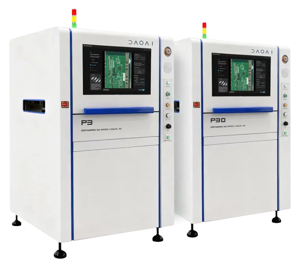
DaoAI P3/P3D
在线式 · 单轨/双轨适用场景高产量 SMT 产线
相机26MP 高速全域快门相机
分辨率10 微米/像素(FOV 38 × 30 毫米)
镜头10MP 远心光学镜头
光源高亮度 RGB 同轴环形多角度 LED
PCB 尺寸50 × 50 – 500 × 825 毫米
PCB 厚度0.3 – 6 毫米
发送带单轨(P3)/ 双轨(P3D)
计算您的 ROI
了解 AI 驱动 AOI 方案能为您节省多少成本
削减人工成本
每条产线每年节省约 5 万至 7 万人民币。
赋能操作员
将设置工作从「仅限编程工程师」转变为「操作员 30 分钟上手」。
最大化设备利用率
将机器闲置时间重新转化为有效生产时间。
年度节省
20万
人民币 – 30万
人民币
人民币 – 30万
人民币
每条产线,每一年。
您的工厂数据
您的年度潜在节省金额
基于您的数据:
每条产线每周 NPI 次数:
每次 NPI 所需工时:
工程师时薪:
SMT 产线数量:
根据您的数据,您目前每年在各条 SMT 产在线的 AOI 编程支出为:
采用 DaoAI 的 AI 解决方案后,您可节省 40% 至 60% 的 AOI 编程时间。这表示:
Conservative
Estimate
(40% time
savings)
to
Optimistic
Estimate
(60% time
savings)
预计年度节省(中值):
联系我们获取详细 ROI 报告 →
离线式 2D AI AOI :DaoAI P1 与 P2 采用先进视觉 AI,实现 PCBA 检测编程自动化。系统直接从样板学习,可自动辨识组件、生成边界框并定义缺陷阈值,将建程时间从数小时缩短至 5 分钟。
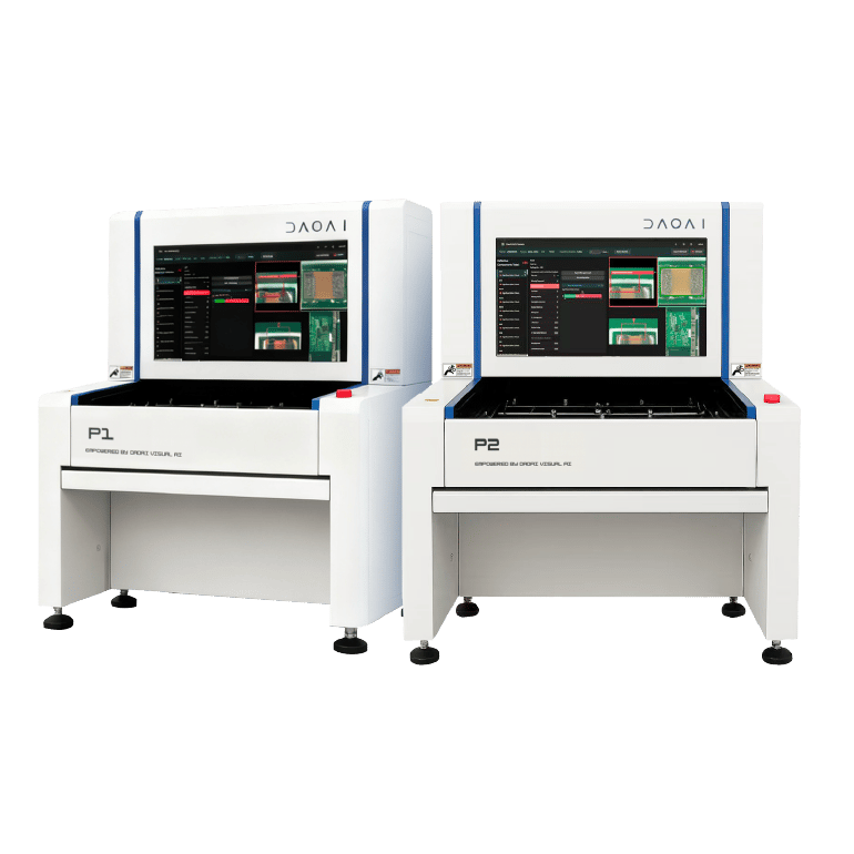
DaoAI P1/P2 规格说明
为速度、精度与适应性而设计
DaoAI P1
5MP 相机
分辨率:15 微米
DaoAI P2
12MP 相机
分辨率:10 微米
DaoAI P1
DaoAI P2
光学系统
相机
5 MP
12MP
Resolution
10 微米
15 微米
光源
Multispectral
ultra-high-speed RGB six-channel
lighting
Multispectral
ultra-high-speed RGB six-channel
lighting
Lens
Dual telecentric
optical lenses
Dual telecentric
optical lenses
输送系统与 PCB 尺寸
PCB Size
0.5×50mm -
470×330mm
0.5×50mm -
470×330mm
PCB Thickness
0.5mm - 5mm
0.5mm - 5mm
Maximum PCB Warpage
Top25mm;Bottom110mm
Top25mm;Bottom110mm
Positioning Accuracy
±3mm
±3mm
Maximum Component Height
2.5mm
2.5mm
检测能力
PCB Size
Missing
components, Reversed components,
Position offset, Polarity errors, Wrong
components, Component damage, Bent
leads, Foreign materials on PCB,
Contaminated or solder-stained gold
fingers, Glue overflow
Missing
components, Reversed components,
Position offset, Polarity errors, Wrong
components, Component damage, Bent
leads, Foreign materials on PCB,
Contaminated or solder-stained gold
fingers, Glue overflow
Solder Joint Inspection
Excess solder /
insufficient solder, Tombstoning, Solder
bridging, Cold solder / poor wetting,
Lifted leads, Solder balls, Post–wave
soldering defects (including
through-hole components)
Excess solder /
insufficient solder, Tombstoning, Solder
bridging, Cold solder / poor wetting,
Lifted leads, Solder balls, Post–wave
soldering defects (including
through-hole components)
Process Coverage
Supports
inspection of solder paste, red-glue
(SMT adhesive), and post–wave soldering
PCB assembly quality
Supports
inspection of solder paste, red-glue
(SMT adhesive), and post–wave soldering
PCB assembly quality
附加功能
Marking Function
PCB Fiducial
Mark, Panel Mark, Break-off Tab Mark
Recognition
PCB Fiducial
Mark, Panel Mark, Break-off Tab Mark
Recognition
Programming Function
CAD Data Import:
Automated region generation and
inspection parameter setupAutomatic
Component Library Indexing
CAD Data Import:
Automated region generation and
inspection parameter setupAutomatic
Component Library Indexing
Logging Function
Statistical
Process Control (SPC) and Data Reporting
Statistical
Process Control (SPC) and Data Reporting
Accessibility
Voice-Controlled
Operation
Voice-Controlled
Operation
检测与自动配置能力
| 组件本体 | 极性 | IC 引脚 | 字符 | |
|---|---|---|---|---|
| 电容 |
|
|
|
|
| 电阻 |
|
|
|
|
| 多层片式电感 |
|
|
||
| 铝电解电容 |
|
|
|
|
| 钽电容 |
|
|
|
|
| 电阻数组 |
|
|
|
|
| 功率电感 |
|
|
||
| LED |
|
|
|
|
|
SOT/SOD |
|
|
|
|
|
SOIC/SOP/TSOP/TSSOP/MSOP |
|
|
|
|
|
QFP |
|
|
|
|
|
QFN |
|
|
||
| TO-263/TO-252 |
|
|