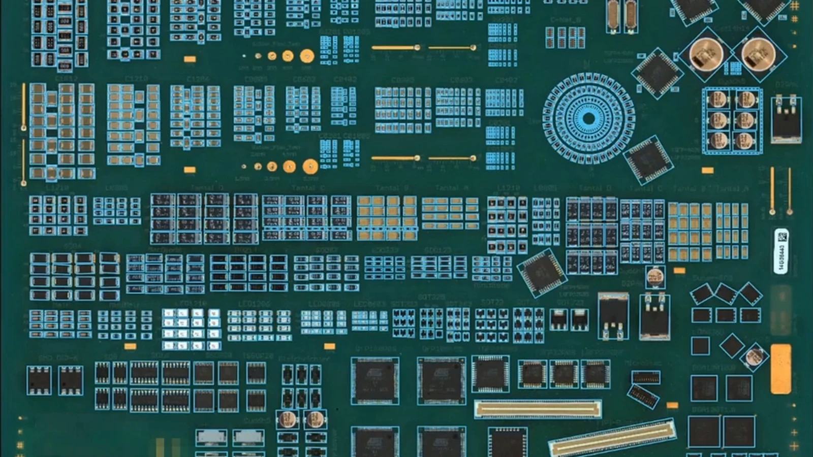
The AOI specification that most decides what a machine can inspect is resolution in micrometers per pixel, because it sets how many pixels land on your smallest component and joint. Field of view (FOV) and FOV time decide how long a board takes to image, while lens type and lighting decide how consistent those images are across the board. Camera megapixels matter only together with FOV: the same sensor spread over a larger area gives coarser resolution.
What does the camera megapixel (MP) figure tell you?
Megapixels are the number of pixels on the camera sensor. On their own they say nothing about how much detail the machine sees, because the optics decide how much board area those pixels cover.
The relationship is simple: resolution (µm per pixel) equals FOV width divided by the number of pixels across the sensor. You can check it on any spec sheet that lists all three numbers.
Take the DaoAI P3 as a worked example. It lists a 26 MP global-shutter camera, 10 µm per pixel and a 51 × 51 mm field of view. At 10 µm per pixel, 51 mm is 5,100 pixels, and 5,100 × 5,100 is about 26 million pixels, so the numbers agree. The P5 lists 10 µm optical resolution over a 50 × 40 mm FOV, which is 5,000 × 4,000 pixels, or 20 MP, close to its 21 MP camera.
If a vendor quotes only megapixels, ask for FOV and resolution before comparing.
What does µm per pixel mean, and how small can a machine inspect?
Micrometers per pixel is the width of board that one pixel covers. At 10 µm per pixel, a 1 mm feature spans 100 pixels; at 15 µm per pixel, the same feature spans about 67 pixels.
What matters is how many pixels land on the smallest thing you need to judge. That is usually not the component body but the termination, the fillet or the gap between two leads. A common rule of thumb is to have at least several pixels across the smallest gap or feature you must detect, and more for reliable solder-fillet judgments.
| Feature | Nominal size | Pixels at 10 µm/px | Pixels at 15 µm/px |
|---|
| 01005 chip (imperial; 0402 metric) | 0.4 × 0.2 mm | 40 × 20 | ≈ 27 × 13 |
| 0201 chip (imperial; 0603 metric) | 0.6 × 0.3 mm | 60 × 30 | 40 × 20 |
| 0402 chip (imperial; 1005 metric) | 1.0 × 0.5 mm | 100 × 50 | ≈ 67 × 33 |
| Lead gap on a 0.3 mm pitch IC (about half the pitch) | ≈ 0.15 mm | ≈ 15 | ≈ 10 |
Watch the naming trap. Chip sizes are quoted in imperial or metric codes, and "0201" means a 0.6 × 0.3 mm part in imperial but a 0.25 × 0.125 mm part in metric. DaoAI's 3D machines avoid the ambiguity by listing "0603 metric, 0201 inch" as the smallest component.
What is field of view (FOV), and how does it affect cycle time?
The field of view is the board area captured in one image. A board larger than the FOV is imaged as a grid of tiles, and the machine moves the camera or the board between them.
The number of tiles sets the imaging time. A P3 with a 51 × 51 mm FOV would need at most 10 × 12 = 120 tiles to cover a full 500 × 600 mm board, before overlap. DaoAI's capture path optimization stops the camera only where the board requires it, so sparse boards need fewer captures.
Vendors quote imaging speed in one of two ways:
- Time per FOV. The DaoAI P1, P1L and P2 list 0.238 seconds per FOV. A board that needs 30 captures would take about 7 seconds to image, before board load and inspection.
- Area per second. The P5 and P5D list over 10 cm² per second. A 100 × 80 mm board is 80 cm², so imaging takes under 8 seconds.
Imaging is only part of cycle time. Ask for the full cycle time on your own board with every check switched on, including board transfer and inspection computation.
Why does a telecentric lens matter for AOI?
A conventional lens sees the edges of its field at an angle, so tall parts near the edge of an image appear to lean outward, and magnification changes with height.
A telecentric lens is designed so its viewing rays are nearly parallel across the field. Telecentric lenses reduce perspective effects and keep magnification nearly constant across changes in object height, which gives the inspection model more consistent images from tile to tile.
The DaoAI P1, P1L and P2 use dual telecentric lenses, and the P3 and P3D use telecentric lenses with a depth of field of 8 to 10 mm. Depth of field matters when low chips and tall parts must both be in focus in one image.
What do lighting channels do?
Solder joints are curved, shiny surfaces, so what the camera sees depends on the angle of the light. AOI machines light the board from several angles, often in different colors, so a fillet's slope shows up as a color pattern.
- Multi-angle RGB lighting separates steep, shallow and flat regions of a joint, which is what fillet and wetting checks rely on. The P1, P1L and P2 use multi-spectral high-speed RGB lighting with 6 channels.
- Coaxial lighting shines along the camera axis and makes flat, reflective surfaces such as pads, markings and component tops read cleanly. The P3 and P3D combine an RGB coaxial ring with multi-angle LED lighting.
- Low-angle lighting picks out edges, leads and raised features. The A3 through-hole machine pairs a high-brightness LED open-aperture flat light with a low-angle light.
What 3D specifications should you compare?
A 3D AOI adds a height map to the color image. The key numbers are height accuracy, measurement range and the number of projection directions.
Height accuracy sets the smallest lift or coplanarity error that can be measured. Measurement range sets the tallest feature that can be measured. More projection directions reduce shadowing behind tall parts. The DaoAI P5 and P5D list ≤ 6 µm height accuracy with the calibration tool, a 25 mm measurement range, and four Scheimpflug structured-light projection units, one per direction.
What board size, thickness and clearance limits apply?
Check these against your largest and thickest products. DaoAI's published figures are reference values, so confirm edge cases on your own boards.
- Board size: minimum and maximum dimensions, and on dual-track machines, the limit per track.
- Thickness: thin flex-rigid boards and thick backplanes are the usual edge cases.
- Clearance and component height: the tallest part allowed above and below the board. The P3 lists 30 mm top and 20 mm bottom clearance; the P5 lists 50 mm top and 40 mm bottom component height. The P1, P1L and P2 have a maximum PCB clearance of 25 mm above the board and 110 mm below it.
- Warpage: how much a board can bend and still be clamped and kept in focus. Ask for this figure separately; it is not the same as clearance.
What should you check on the conveyor?
For inline machines, confirm conveyor height, track count and double-sided handling. The P3 and P3D run at a conveyor height of 900 ± 25 mm and switch between top-side and bottom-side programs automatically; the P5 and P5D run at 900 ± 20 mm.
The offline P1, P1L and P2 have no conveyor; boards are loaded by hand and clamped automatically.
DaoAI machine specifications as worked examples
| Spec | P1 / P1L | P2 | P3 / P3D | P5 / P5D | A3 |
|---|
| Camera | 5 MP | 12 MP | 26 MP, global shutter | 21 MP high-speed | 26 MP color |
| Resolution | 15 µm/px | 10 µm/px | 10 µm/px | 10 µm optical; ≤ 6 µm height | Not listed |
| Field of view | Not listed | Not listed | 51 × 51 mm | 50 × 40 mm | Not listed |
| Lens | Dual telecentric | Dual telecentric | Telecentric, 8–10 mm depth of field | Not listed (3D: four Scheimpflug projectors) | 18 mm industrial |
| Lighting | RGB, 6 channel | RGB, 6 channel | RGB coaxial ring + multi-angle LED | Not listed | Flat light + low-angle light |
| Speed | 0.238 s per FOV | 0.238 s per FOV | < 1 ms inference per component | > 10 cm²/s | Not listed |
| Max board | 470 × 330 mm / 680 × 510 mm | 470 × 330 mm | 500 × 600 mm / 500 × 325 mm per track | 500 × 600 mm / 500 × 300 mm per track | 420 × 420 mm |
| Board thickness | 0.5–5 mm | 0.5–5 mm | 0.3–6 mm | 0.6–5 mm | Not listed |
| Smallest component | Not listed | Not listed | 0201 (imperial); 0.3 mm pitch ICs; 01005 optional | 0603 metric (0201 inch) | Not listed |
These are reference values, not guaranteed limits. See the P3 and P5 pages for the complete published specifications; the P5 and P5D are available for delivery now.
Which specs matter most for 01005 and 0201 components?
For the smallest chips, resolution comes first. At 10 µm per pixel a 01005 body is about 40 × 20 pixels, while at 15 µm it drops to roughly 27 × 13, leaving few pixels for the terminations and fillets. Depth of field and lighting come next, because tiny joints need to be sharp and evenly lit in every tile.
On the DaoAI range, for 0201 or 01005 chips (imperial sizes), the inline P3 and P3D list 0201 and 0.3 mm pitch ICs, with 01005 available as an option. Whatever the spec sheet says, qualify small-component inspection on your own boards; our guide on evaluating an AI AOI system covers how to run that test.
FAQ
Is a higher-megapixel AOI camera always better?
No. Megapixels only describe the sensor. Resolution in µm per pixel, which depends on both the sensor and the field of view, is what determines the smallest feature the machine can judge.
What resolution do I need to inspect 01005 components?
Finer is better. At 10 µm per pixel, a 01005 chip (0.4 × 0.2 mm) spans about 40 × 20 pixels. Confirm the vendor supports 01005 on the specific model and test with your own boards.
What is a telecentric lens in AOI?
A lens whose viewing rays are nearly parallel across the field. Telecentric lenses reduce perspective effects and keep magnification nearly constant across changes in object height.
How is AOI inspection speed specified?
Usually as time per field of view, such as 0.238 seconds per FOV, or as area per second, such as over 10 cm² per second. Total cycle time also includes board transfer and inspection computation.
Spec sheets narrow the list; your own board settles it. Send us one of your own boards and we will test it for you, free of charge, or book a demo to review the images and results with an engineer.