Solder Balls on PCBA: Causes, Detection and Prevention
Solder balls are stray spheres of solder that can short a board in service. Here is what causes them, why component-based AOI can miss them, and how to prevent them.
2026年9月28日
A solder bridge is unintended solder between adjacent pads or leads that shorts the circuit. Here is what causes it, how each inspection method finds it, and how to prevent it.
A solder bridge is an unintended solder connection between two adjacent pads, leads or terminations that should be electrically isolated, which creates a short circuit on the assembled board. It is most common on fine-pitch parts such as QFPs, SOICs, QFNs and connectors, where the gap between neighboring pads is small enough for excess or slumped solder paste to join during reflow.
Bridging comes down to too much solder in the wrong place before reflow, or molten solder free to flow where it should not:
The same slump and excess paste that bridge fine-pitch leads also throw off stray spheres of solder, so lines fighting bridges often see solder balls as well.
Manual inspection works on coarse pitch but becomes unreliable at fine pitch as operators tire, and bridges under a component body cannot be seen at all.
SPI (solder paste inspection) cannot see a bridge, because bridges form in reflow. It does see the precursors: bridged paste, excess volume and offset deposits, and stopping those boards before placement is the cheapest fix.
2D AOI is the standard post-reflow check for visible bridges between gull-wing leads and chip terminations, where a bridge shows as continuous solder across the gap. 3D AOI adds height, which helps separate a real solder bridge from flux residue or a reflection that only looks like one in a 2D image. AXI (automated X-ray inspection) is needed for hidden joints: BGAs, QFN center pads and other bottom-terminated components.
Electrical test (in-circuit, flying probe or functional test) finds shorts that visual inspection missed, including hidden ones, but only on the nets it covers, and only after the board has passed through the rest of the line.
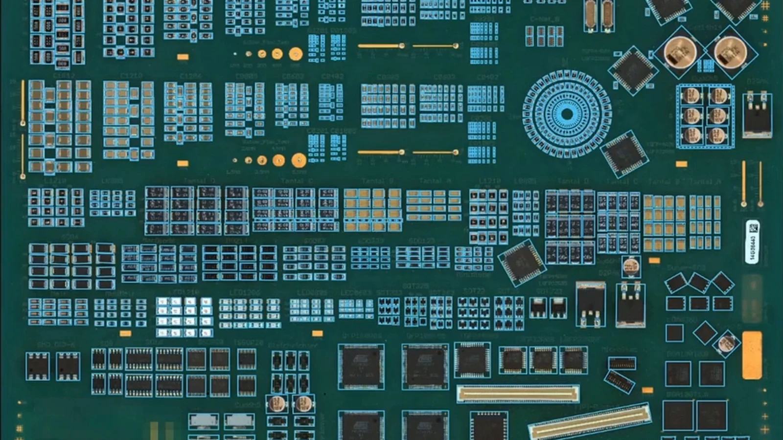
Solder bridging is item 08 in DaoAI's inspection coverage: unintended solder connections between adjacent pads or leads, including on QFP packages. Bridges between adjacent through-hole pads after wave soldering are a separate check, item 13, which runs in post-wave inspection on the A3 and in DIP / through-hole inspection on the P3 and P5. When the machine writes the inspection program from one golden board, AI auto-programming generates the pad, pin and bridge regions itself, and you choose per package type whether bridge regions are inspected, generated only, or skipped.
False calls are the usual reason bridge checks get switched off. On DaoAI, operator feedback teaches the model which variations are acceptable, while solder bridges remain inspection targets.
A bridge under a BGA, QFN or other bottom-terminated part cannot be reached with an iron: the part has to be removed and replaced on a rework station. Log every bridge location: repeat bridges at the same leads point to the stencil, print or wave process, not to the operator.
Fix bridging at the printer first, because most causes show up in SPI data before placement. Check values against your paste datasheet and stencil supplier.
| Cause | Prevention |
|---|---|
| Paste slump | Use paste within its stencil life, follow the supplier's storage and warm-up rules, and keep the printer environment at the recommended temperature and humidity. |
| Excess paste volume on fine pitch | Reduce the aperture relative to the pad, or step down stencil thickness (for example 100 µm / 4 mil instead of 127 µm / 5 mil) while keeping the area ratio at or above 0.66 for good release. |
| Smeared or offset print | Verify stencil-to-board alignment and board support, increase under-stencil wipe frequency, and run the lowest squeegee pressure that still clears the stencil. |
| Hot slump in reflow | Keep the preheat ramp moderate (typically 1–3 °C/s) and keep time above liquidus inside the paste datasheet window. |
| Placement force or offset | Check placement force and Z height per nozzle, and watch AOI offset trends for parts drifting toward one side. |
| Pad and mask design | Keep a solder mask web between fine-pitch pads where the fabricator can hold it, and review pad dimensions against the component datasheet. |
| Wave solder bridges on through-hole leads | Check flux coverage and preheat, conveyor speed and angle, and lead protrusion, and add solder thieves at the trailing pins of connector rows. |
If bridges are slipping past your current inspection, or bridge checks raise so many false calls that they get turned off, send us one of your own boards and we will test it for you, free of charge.
A solder bridge is one physical cause of a short: solder joining two conductors that should be isolated. Shorts can also come from debris, bare-board defects or misplaced parts.
SPI cannot see a bridge, which forms during reflow, but it catches the causes: bridged paste after printing, excess volume and offset deposits. Holding those boards before placement prevents most print-related bridges.
No. Optical inspection only sees what is visible from above, so bridges under a component body need X-ray inspection (AXI), while AOI covers bridges between visible leads and terminations.
Apply flux, then drag a clean, tinned iron tip along the leads or lift the excess with solder wick, and re-inspect. Bridges under a BGA or QFN need the part removed with a rework station. If the same location bridges repeatedly, fix the stencil, print or wave process instead.
Solder balls are stray spheres of solder that can short a board in service. Here is what causes them, why component-based AOI can miss them, and how to prevent them.
2026年9月28日
DaoAI vs Nordson YESTECH AOI: golden-board vs CAD-and-library programming, inline 3D, through-hole, on-machine AI, and how to test both on your boards.
2026年10月7日
DaoAI vs CyberOptics (Nordson) SQ-series 3D AOI: golden-board vs library-based programming, inline 3D, through-hole, on-machine AI and how to test both.
2026年10月7日
AI検査の知見、製品ニュース、業界分析。月一回、必要な情報だけをお届け。
お問い合わせへの回答のためにお客様の情報を使用します。 プライバシーポリシーをご確認ください。