
多品種少量PCB実装向けAOIの選び方
スペックは単なる入場券に過ぎません。多品種少量の製造現場における真の差は、プログラミング入力、段取り替え時間、そして誤報負荷です。7つの質問がその実態を明らかにします。
2026年8月5日
SPI checks paste after printing, AOI checks the visible board after placement or soldering, and AXI checks hidden joints. What each sees, what it misses and where it belongs on your line.
SPI (solder paste inspection) checks the paste deposit right after the printer, AOI (automated optical inspection) checks what can be seen on the board after placement, reflow or wave soldering, and AXI (automated X-ray inspection) checks joints hidden under components. Most SMT lines use SPI and AOI as the backbone and add AXI only where boards carry BGAs, QFNs or other hidden joints that need it. DaoAI makes AOI machines only (offline 2D, inline 2D, inline 3D and through-hole), which take the AOI position next to the SPI and X-ray equipment a line already runs.
The three are complementary, not competing. Each sees defects the others cannot, and each sits at a different point in the line. This guide lays out what each one sees, what it misses, and where it belongs.
SPI measures solder paste on the bare board after stencil printing, usually with a 3D height sensor. It reports volume, height, area and offset for each deposit, plus bridging and missing paste. It is the earliest and cheapest place to catch a solder problem: a bad print can be cleaned and reprinted before any components are placed.
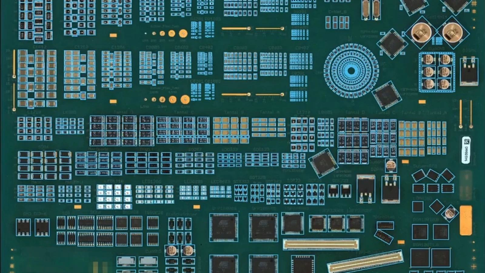
AOI uses cameras and multi-angle lighting to judge the visible board: components (present, correct, shifted, rotated, reversed), markings, and the visible solder fillets and leads. A 2D AOI works from color images; a 3D AOI adds measured height, so lifted leads, coplanarity and solder volume are measured rather than inferred.
AXI passes X-rays through the assembly and images the density of solder, including joints under the component body. It is the method for BGA and QFN joints, voids, head-in-pillow, and internal through-hole barrel fill. It is slower and more expensive per board than AOI, and it cannot read markings or check colors.
| SPI | AOI (2D / 3D) | AXI | |
|---|---|---|---|
| How it sees | 3D height measurement of paste deposits | Color images under multi-angle light; 3D adds structured-light height | X-ray transmission (2D, 2.5D or CT) |
| Typical line position | Post-print, before placement | Pre-reflow, post-reflow, pre-wave or post-wave | Post-reflow, often offline or sampled |
| Main defects covered | Insufficient or excess paste, height, area, offset, paste bridging, missing deposits | Missing, wrong, shifted, rotated, reversed, tombstoned or damaged parts; markings; visible solder joints, bridges, lifted leads; solder balls and debris | BGA/QFN/LGA joints, voids, head-in-pillow, hidden bridges, through-hole barrel fill |
| What it misses | Anything after placement: components, polarity, reflow defects | Joints hidden under component bodies; internal voids | Color, markings, polarity marks on the body; poor at lightweight or non-metallic features |
| Relative cycle time | Fast; keeps up with the printer | Fast; keeps up with the line inline | Slower; often used on a sample or on selected parts |
SPI goes directly after the stencil printer. A large share of solder defects start at printing, and at this stage there is no component on the board, so the fix costs little. SPI data can also feed back to the printer to correct offset and trigger stencil cleaning.
An AOI after the pick-and-place machine and before the reflow oven checks for missing, shifted, wrong or reversed components while they can still be corrected by hand. It cannot judge solder joints, because they have not formed yet. Lines with expensive boards or high placement risk use it; many lines skip it and rely on post-reflow AOI.
Post-reflow AOI is the most common position and covers the widest range of defects: component presence and position, polarity, markings, visible joints, bridges, tombstones, lifted leads, solder balls and foreign objects. If the board carries BGAs or bottom-terminated parts, AXI follows AOI for those joints, sometimes on a sampling basis.
On mixed-technology boards, an AOI before the wave solder machine checks that through-hole parts are inserted, present, correct and the right way round. After the wave, AOI checks the visible solder side for missing, insufficient or excess solder and bridges between pins.
Not necessarily. A practical order of priority looks like this:
Start from your defect Pareto: which defects reach test, rework or the customer, and which inspection could have seen them.
DaoAI makes AOI machines only. We do not sell SPI or AXI. A DaoAI machine takes the AOI position on your line, next to the SPI and X-ray equipment you already run, and exports its results to your MES as CSV.
| DaoAI machine | Type | Where it fits | Key imaging spec |
|---|---|---|---|
| P3 / P3D | Inline 2D, single / dual track | In the SMT conveyor line | 26 MP global shutter, 10 µm/px |
| P5 / P5D | Inline 3D, single / dual track | In the SMT line, where height data matters | 21 MP, 10 µm optical, ≤ 6 µm height accuracy |
| A3 | Through-hole, bench-top straddle | Over the existing line; one machine for pre-wave and post-wave | 26 MP, 420 × 420 mm max board |
| P1 / P1L / P2 | Offline 2D, manual load | Beside the line: NPI, short runs, labs | 5 MP at 15 µm/px (P1, P1L); 12 MP at 10 µm/px (P2) |
The P3 and P5 also support DIP/through-hole inspection, and the P5 and P5D inline 3D models are available for delivery now.
Every DaoAI machine runs the same core AI software. Auto-programming writes the inspection program from one golden board in 30 seconds to 5 minutes, with no CAD file required; DaoAI auto-programming does not require a prebuilt component library. The 16 inspection capabilities, from polarity and bridging to solder balls and foreign objects, are listed on the inspection coverage page.
No. 3D AOI measures height on the finished, visible assembly, which improves judgement of lifted leads, coplanarity and solder volume on visible joints. It does not see paste before placement, as SPI does, and it cannot see through a component body to a hidden joint, as AXI does.
SPI measures solder paste deposits after printing, before any components are placed. AOI inspects the board after placement or soldering, checking components, markings and visible solder joints.
No. BGA joints sit under the component body, out of sight of any camera. AXI is the method for BGA, QFN and other hidden joints; AOI can still check the BGA's presence, position and markings.
The most common position is after the reflow oven, where AOI sees the finished joints. Some lines add a second AOI after placement, before reflow, to catch placement errors while they are cheap to fix.
No. DaoAI makes AOI machines only: offline 2D, inline 2D, inline 3D and through-hole models. They work alongside your existing SPI and AXI equipment.
If you are deciding where an AOI belongs on your line, start with your own product. Send us one of your own boards and we will test it for you, free of charge, and an engineer will tell you which machine and position it needs.
スペックは単なる入場券に過ぎません。多品種少量の製造現場における真の差は、プログラミング入力、段取り替え時間、そして誤報負荷です。7つの質問がその実態を明らかにします。
2026年8月5日
DaoAI vs Nordson YESTECH AOI: golden-board vs CAD-and-library programming, inline 3D, through-hole, on-machine AI, and how to test both on your boards.
2026年10月7日
DaoAI vs CyberOptics (Nordson) SQ-series 3D AOI: golden-board vs library-based programming, inline 3D, through-hole, on-machine AI and how to test both.
2026年10月7日
AI検査の知見、製品ニュース、業界分析。月一回、必要な情報だけをお届け。
お問い合わせへの回答のためにお客様の情報を使用します。 プライバシーポリシーをご確認ください。