Automated optical inspection (AOI) photographs an assembled circuit board under controlled lighting and checks what it sees against what should be there. It confirms that every component is present, correct, the right way round and in the right place. It also checks that every visible solder joint has the right shape, with no bridges, no starved joints and no lifted leads. AOI cannot see through things. Joints hidden under a BGA or a QFN and solder inside a through-hole barrel need X-ray, and whether a part actually works needs electrical test.
This guide walks through the main defect families: what each one is, what it causes, where it usually comes from, and whether AOI can catch it. Each section links to a deeper article if you need the detail.
Defect, process indicator or acceptable?
Not everything that looks imperfect is a defect. Most electronics manufacturers judge assembled boards against IPC-A-610, which sets criteria for three product classes [1]:
- Class 1, General Electronic Products: the main requirement is that the assembly works.
- Class 2, Dedicated Service Electronic Products: continued performance and extended life are required; uninterrupted service is desired but not critical.
- Class 3, High Performance/Harsh Environment Electronic Products: the equipment must work on demand and downtime cannot be tolerated, as in life-support systems.
The customer or contract sets the class, not the inspector. The same joint can be acceptable on a Class 1 board and a defect on a Class 3 board.
Within a class, a condition falls into one of three groups [2]:
- Acceptable: not necessarily perfect, but it maintains the integrity and reliability of the assembly in service.
- Process indicator: not a defect and does not affect form, fit or function, but it shows the result is not fully meeting the acceptance criteria, so the process should be monitored.
- Defect: fails the acceptance criteria, or may not ensure form, fit or function in the end-use environment. The manufacturer must record each defect and decide what to do with it (rework, repair, scrap or use as is; repair and use as is may need the customer's agreement).
Recent revisions dropped the old "target" (ideal) condition [2].
This matters for AOI. The machine flags deviations, and your acceptance criteria decide which flags are defects. A program tuned tighter than your class floods operators with calls on acceptable joints. A program tuned too loosely lets real defects through.
The main defect families
1. Missing, wrong or extra component
- What it is: a part that was not placed, the wrong part or value, or a part on a position that should be empty.
- Why it matters: the circuit fails or behaves out of spec. A wrong value may still power up and pass a quick check.
- Common causes: pick-up errors, a wrong or empty reel after changeover, parts knocked off before reflow, an unapproved alternate.
- Can AOI see it? Missing and extra parts: yes. Wrong part: partly. AOI compares size, colour and printed markings (OCR/OCV), but most small ceramic capacitors carry no marking, so their value needs electrical test.
More: Missing and wrong components · OCR and OCV for component markings
2. Polarity and orientation
- What it is: a diode, polarized capacitor or IC placed reversed or rotated.
- Why it matters: the circuit may not work, and the part may be damaged at power-up.
- Common causes: wrong rotation in the placement program, a tray or tube loaded the wrong way round, parts oriented differently in the tape by another supplier, and alternate parts whose polarity mark differs from the original [4].
- Can AOI see it? Yes, when the part has a visible mark (notch, band, dot or bevel). X-ray mostly cannot, because it sees solder and metal rather than the component body [4].
More: Reversed polarity components
3. Shift, skew and rotation
- What it is: a part sitting off-centre or twisted on its pads.
- Why it matters: less solder contact; at the extreme, an open joint, or a fine-pitch lead touching its neighbour's pad.
- Common causes: placement offset, paste printed off the pads, the board being jolted before reflow, uneven paste or heating pulling the part during reflow.
- Can AOI see it? Yes. AOI measures position against the pads; how much overhang is allowed depends on your class.
More: Component shift and skew
4. Tombstoning and billboarding
- What it is: a small chip part standing up on one end (tombstone) or lying on its side (billboard).
- Why it matters: a tombstone is an open circuit. A billboarded part has less solder contact and is judged against class-specific criteria.
- Common causes: unequal soldering forces on the two ends, from uneven heating (for example, one pad tied to a ground plane), uneven placement on the pads, or marginal solderability [3].
- Can AOI see it? Yes. Both change the part's outline and height.
More: Tombstoning
5. Solder bridging (shorts)
- What it is: solder joining two conductors that should be separate.
- Why it matters: a short circuit [3]. The board fails test, or parts are damaged at power-up.
- Common causes: too much paste (large apertures or a thick stencil), paste slumping before or during reflow, paste bleeding under the stencil, excessive placement pressure or misalignment [3].
- Can AOI see it? Yes, on visible leads. Bridges under BGAs and bottom-terminated parts need X-ray. ICT also catches shorts between nets it can reach.
More: Solder bridges
6. Insufficient solder and open joints
- What it is: too little solder to form a complete joint, or no connection at all.
- Why it matters: an open circuit, or worse, a weak joint that passes test and cracks later under temperature cycling or vibration, causing intermittent field failures. Fillet shape matters for joint life too: for leadframe-based bottom-terminated parts such as QFNs, one study reports that the number of thermal cycles to failure is typically up to about 25% lower when there is no outer, visible fillet [5].
- Common causes: squeegee scooping paste out of apertures, clogged apertures, print speed or paste viscosity, solder wicking up a lead that heats faster than the pad, solder mask on the pad, poor solderability [3].
- Can AOI see it? On visible joints, yes or partly; 3D height measurement helps. On hidden joints, no. Looking straight down at a standard QFN, a pin wetted only underneath looks the same as one not wetted at all [5].
More: Insufficient solder · Open solder joints
7. Lifted leads
- What it is: a pin of a leaded IC sitting above its pad instead of in the solder.
- Why it matters: an open or weak joint that may make contact at test and fail later.
- Common causes: bent leads from handling, poor lead coplanarity, and board or package warpage in reflow. Solder wicking up the lead can also leave the joint open [3].
- Can AOI see it? Partly with a single top-down camera, because a small lift is hard to see from directly above. Angled views or 3D height measurement do better.
More: Lifted leads and coplanarity
8. Solder balls, splash and foreign material
- What it is: small solder spheres on the board, larger beads beside chip parts, spatter, or debris.
- Why it matters: loose balls and debris can move in service and short conductors. Acceptance depends on whether they are attached or entrapped and on electrical clearance; check your IPC-A-610 revision.
- Common causes: oxidized or old paste, paste left too long before reflow, reflow ramp too slow (balling, beading) or too fast (spatter), too much paste, paste bleeding under the stencil [3].
- Can AOI see it? Yes, for visible balls and debris above the system's resolution. Not under component bodies.
More: Solder balls
9. Excess solder
- What it is: a bulging joint where the lead outline is buried in solder [3].
- Why it matters: not always a defect in itself, but it can hide whether the lead wetted, and it raises bridging risk at fine pitch. Check your class criteria, for example the limits on solder touching the component body.
- Common causes: too much paste from stencil thickness, aperture design, squeegee pressure, snap-off or bleed-out [3].
- Can AOI see it? Yes; 3D height measurement makes it more reliable.
10. Component damage and markings
- What it is: cracked or chipped bodies, damaged terminations, missing or wrong markings.
- Why it matters: damaged parts can pass test and fail later. A wrong marking can mean a wrong part.
- Common causes: board flexing during depaneling, fixturing or screw-down, handling, placement force. Plastic packages that absorb moisture can crack during reflow, which is why IPC/JEDEC J-STD-020 classifies moisture sensitivity and J-STD-033 governs handling [1].
- Can AOI see it? Partly. Visible chips, cracks and markings (via OCR/OCV): yes. Internal damage: no. Production X-ray is set up to image solder and metal, so it rarely shows body cracks or markings either [4].
More: OCR and OCV for component markings
11. Through-hole joints
- What it is: problems on leaded parts soldered by wave, selective or hand soldering, including poor hole fill, bridges, missing fillets and unsoldered pins.
- Why it matters: the same opens and shorts as SMT, often on connectors and power parts that also carry mechanical load.
- Common causes: wave or selective settings (flux, preheat, solder temperature, contact time), lead-to-hole fit, and heavy copper planes drawing heat away.
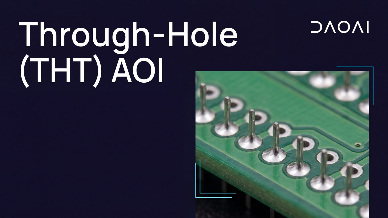
- Can AOI see it? Only from the sides it can see. AOI checks fillets and bridges on the solder side and presence and polarity on the component side. It cannot measure how far solder rose inside the barrel. The general minimum for Class 2 and 3 assemblies is 75% fill (the standard allows limited Class 2 exceptions), and an oblique X-ray view shows it [6].
More: Through-hole AOI inspection
A note on hidden joints
On BGAs, LGAs and other parts whose joints sit under the body, AOI can at best confirm position and polarity [4]. The same applies to the part of a J-lead joint that is tucked under the package. Standard QFNs are a special case. Their cut lead ends are bare copper that does not reliably wet, so an outer fillet does not reliably form, and a top-down camera cannot judge the joint [5]. "Wettable-flank" QFNs are designed to show a fillet AOI can check [5]. Otherwise, use X-ray.
Summary table
| Defect |
What it can cause |
Typical process cause |
Best detection method |
| Missing / extra part |
Circuit fails |
Pick-up error, feeder or reel setup |
AOI |
| Wrong part or value |
Out-of-spec behaviour |
Wrong reel, unapproved alternate |
AOI with OCR/OCV (marked parts); ICT (unmarked passives) |
| Reversed polarity |
Failure or damage at power-up |
Program rotation, tray or tape orientation, alternate marks |
AOI |
| Shift / skew |
Weak joint, open or short |
Placement or print offset, vibration |
AOI |
| Tombstone / billboard |
Open circuit (tombstone); reduced solder contact (billboard) |
Uneven heating or placement, solderability |
AOI |
| Bridge |
Short circuit |
Excess paste, slump, bleed, placement |
SPI (cause), AOI; AXI if hidden; ICT |
| Insufficient / open |
Open or intermittent joint, shorter fatigue life |
Printing, wicking, solderability |
SPI (cause), AOI (3D helps); AXI if hidden |
| Lifted lead |
Open or intermittent joint |
Bent leads, coplanarity, warpage |
Angled-view or 3D AOI |
| Solder balls / debris |
Later shorts |
Paste condition, ramp rate, print bleed |
AOI |
| Excess solder |
Hidden wetting, bridging risk |
Too much paste |
SPI (cause), AOI |
| Body damage / marking |
Latent failure, wrong part |
Board flex, handling, moisture |
AOI (visible damage and markings only) |
| Through-hole fill |
Weak or open joint |
Wave or selective settings |
AOI (fillets), X-ray (fill) |
| Hidden-joint defects (BGA, QFN underside) |
Opens, shorts, intermittents |
Printing, profile, warpage |
AXI |
Where AOI sits in the line
A typical SMT line runs print → SPI → placement → reflow → AOI, followed by through-hole soldering and test. Each inspection step has its own job, and few lines use all of them.
- SPI (solder paste inspection) measures paste deposits before any part is placed. A bad print can be cleaned and reprinted cheaply, which makes SPI the best place to stop many bridges and opens at their cause.
- Pre-reflow AOI (optional) checks placement before soldering, giving fast feedback to the placement machine [4].
- Post-reflow AOI is the main check of placement and visible solder joints.
- AXI (automated X-ray) inspects hidden joints. One established setup runs AOI across the whole board and limits X-ray to the hidden joints [4].
- Post-wave or post-selective AOI checks the through-hole solder side.
- ICT or flying probe tests electrically for shorts, opens and component values.
- Functional test confirms the board actually does its job.
No single method covers every defect. Combining methods closes each other's gaps [4]. See AOI vs SPI vs AXI for a side-by-side comparison.
FAQ
What does AOI check on a PCB?
Component presence, identity (by appearance and markings), polarity and position, plus the shape of visible solder joints: bridges, insufficient solder, lifted leads, tombstones, solder balls and excess solder.
Can AOI find every assembly defect?
No. It cannot see hidden joints (BGA, LGA, standard QFN undersides), solder inside through-hole barrels, the value of unmarked parts, or whether a part works. Those need X-ray, electrical test or functional test.
What is the difference between AOI, SPI and AXI?
SPI inspects solder paste before placement. AOI inspects placed parts and visible joints optically. AXI uses X-ray to inspect joints AOI cannot see.
Is every AOI call a defect?
No. Some calls are false calls on acceptable joints, and some flag process indicators that need watching rather than rework. Your IPC-A-610 class and customer criteria decide.
Which IPC-A-610 class applies to my board?
The customer or contract specifies it. Class 2 fits products that need extended life where uninterrupted service is desired but not critical; Class 3 fits products where downtime cannot be tolerated [1].
Send us one of your own SMT boards and we will test it for you, free of charge. Talk to an engineer.
Sources
- Global Electronics Association (IPC), "IPC Standards Guidance for Printed Board Assemblies," 2026 revision. Classification section (Class 1/2/3 definitions) and standards list (J-STD-020, J-STD-033). https://www.electronics.org/media/12451/download
- L. Lambert, "The Death of the Target Condition," Circuits Assembly, October 2022. https://circuitsassembly.com/ca/features-itemid-fix/38106-the-death-of-the-target-condition.html
- AIM Solder, "SMT Troubleshooting" guide (solder balling, beading, bridging, opens/insufficient, tombstoning, excess solder, non-wetting). https://aimsolder.com/sites/default/files/documents/smt_ts.pdf
- G. Struthers, "AOI/AXI Combinational Inspection Strategy," IPC SMEMA Council APEX 2002. https://www.electronics.org/system/files/technical_resource/E20%2600011.pdf
- U. Welzel et al. (Robert Bosch GmbH), "Wettable-Flanks: Enabler for the Use of Bottom-Termination Components in Mass Production of High-Reliability Electronic Control Units," IPC APEX EXPO technical paper. https://www.electronics.org/system/files/technical_resource/E40%26S05_02%20-%20Udo%20Welzel.pdf
- D. Bernard, "Clarifying Through-Hole Fill Levels," Circuits Assembly, October 2019. https://circuitsassembly.com/ca/features-itemid-fix/415-test-and-inspection/32304-clarifying-through-hole-fill-levels.html